PCB Routing Showcase
Routing around high-power copper areas
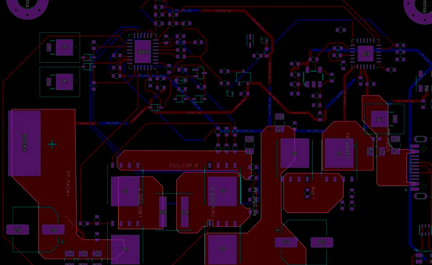
A real PCB visual focused on the relationship between high-current copper, signal traces, and component zones, useful for solution review, board-level coordination, and pre-production checks.
Thermal and chip boundary
High-current copper path
Signal detour and isolation
4L
Multi-layer routing and power-zone separation
18A
Copper planning for high-current paths
6mil
Fine-pitch signal routing and component clearance